- 您现在的位置:买卖IC网 > Sheet目录17346 > MIC58P42BWM (Micrel Inc)IC DRVR LATCH 8BIT SER IN 18SOIC
�� �
�
�MIC58P42�
�CLOCK�
�DATA� IN�
�A�
�B�
�D�
�Micrel�
�E�
�F�
�STROBE�
�C�
�OUTPUT�
�ENABLE�
�G�
�OUT� N�
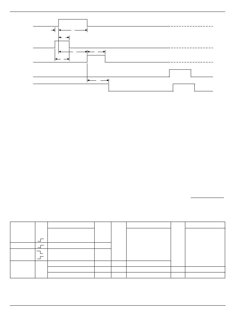
�Timing� Conditions�
�(T� A� =� +25� °� C,� Logic� Levels� are� V� DD� and� V� SS� ),� V� DD� =� 5V�
�A.�
�B.�
�C.�
�D.�
�E.�
�F.�
�G.�
�Typical� Data� Active� Time� Before� Clock� Pulse� (Data� Set-Up� Time)� ...........................................................................� 75� ns�
�Minimum� Data� Active� Time� After� Clock� Pulse� (Data� Hold� Time)� ..............................................................................� 75� ns�
�Minimum� Data� Pulse� Width� .....................................................................................................................................� 150� ns�
�Minimum� Clock� Pulse� Width� ....................................................................................................................................� 150� ns�
�Minimum� Time� Between� Clock� Activation� and� Strobe� .............................................................................................� 300� ns�
�Minimum� Strobe� Pulse� Width� ...................................................................................................................................� 100� ns�
�Typical� Time� Between� Strobe� Activation� and� Output� Transition� .............................................................................� 500� ns�
�SERIAL� DATA� present� at� the� input� is� transferred� to� the� shift� register� on� the� logic� “0”� to� logic� “1”� transition� of� the� CLOCK� input�
�pulse.� On� succeeding� CLOCK� pulses,� the� registers� shift� data� information� towards� the� SERIAL� DATA� OUTPUT.� The� SERIAL�
�DATA� must� appear� at� the� input� prior� to� the� rising� edge� of� the� CLOCK� input� waveform.�
�Information� present� at� any� register� is� transferred� to� its� respective� latch� when� the� STROBE� is� high� (serial-to-parallel� conversion).�
�The� latches� will� continue� to� accept� new� data� as� long� as� the� STROBE� is� held� high.� Applications� where� the� latches� are� bypassed�
�(STROBE� tied� high)� will� require� that� the� ENABLE� input� be� high� to� prevent� invalid� output� states.�
�When� the� ENABLE� input� is� high,� all� of� the� output� buffers� are� disabled� (OFF)� without� affecting� information� stored in the latche� s�
�or� shift� register.� With� the� ENABLE� input� low,� the� outputs� are� controlled� by� the� state� of� the� latches.� A� positive� OUTPUT� ENABLE/�
�RESET� pulse� resets� the� output� after� a� current� shutdown� fault.� Thermal� limit� faults� are� not� latched� and� require� no� reset� pulse.�
�MIC58P42� Truth� Table�
�Shift� Register� Contents�
�Serial�
�Latch� Contents�
�Output� Contents�
�Serial� Data�
�Clock�
�Data�
�Strobe�
�Output�
�Input�
�Input�
�I� 1�
�I� 2�
�I� 3� ……�
�I� 8�
�Output�
�Input�
�I� 1�
�I� 2�
�I� 3�
�……�
�I� 8� Enable� I� 1�
�I� 2�
�I� 3�
�……� I� 8�
�H�
�L�
�X�
�H�
�L�
�R1�
�O�
�R� 1�
�R� 1�
�R2�
�O�
�R� 2� ……�
�R� 2� ……�
�R� 3� ……�
�O� ……�
�R� 7�
�R� 7�
�R� 8�
�O�
�R� 7�
�R� 7�
�R� 8�
�L�
�X�
�X�
�X� ……�
�X�
�X�
�L�
�R� 1� R� 2�
�R� 3�
�……�
�R� 8�
�P� 1�
�P� 2�
�P� 3� ……�
�P� 8�
�P� 8�
�H�
�P� 1� P� 2�
�P� 3�
�……�
�P� 8�
�L�
�P� 1�
�P� 2�
�P� 3� ……P� 8�
�X�
�X�
�X�
�……�
�X�
�H�
�H�
�H�
�H� ……� H�
�L� =� Low� Logic� Level�
�H� =� High� Logic� Level�
�X� =� Irrelevant�
�P� =� Present� State�
�R� =� Previous� State�
�O� =� Output� OFF�
�7-52�
�October� 1998�
�发布紧急采购,3分钟左右您将得到回复。
相关PDF资料
A9CAG-1408F
FLEX CABLE - AFG14G/AF14/AFE14T
TAC475K015P02-F
CAP TANT 4.7UF 15V 10% AXIAL
A9CAG-1305F
FLEX CABLE - AFG13G/AF13/AFE13T
A9BAG-1408F
FLEX CABLE - AFF14G/AF14/AFE14T
RBM06DRTS
CONN EDGECARD 12POS DIP .156 SLD
A9CAG-1606F
FLEX CABLE - AFG16G/AF16/AFE16T
RS3-2405SZ/H3
CONV DC/DC 3W 9-27VIN 05VOUT
RB-053.3D/H
CONV DC/DC 1W 5VIN +/-3.3VOUT
相关代理商/技术参数
MIC58P42BWM TR
功能描述:闭锁 8-Bit Serial Input Protected Latched Driver
RoHS:否 制造商:Micrel 电路数量:1 逻辑类型:CMOS 逻辑系列:TTL 极性:Non-Inverting 输出线路数量:9 高电平输出电流: 低电平输出电流: 传播延迟时间: 电源电压-最大:12 V 电源电压-最小:5 V 最大工作温度:+ 85 C 最小工作温度:- 40 C 封装 / 箱体:SOIC-16 封装:Reel
MIC58P42YN
功能描述:闭锁 8-Bit Serial Input Protected Latched Driver (Lead Free)
RoHS:否 制造商:Micrel 电路数量:1 逻辑类型:CMOS 逻辑系列:TTL 极性:Non-Inverting 输出线路数量:9 高电平输出电流: 低电平输出电流: 传播延迟时间: 电源电压-最大:12 V 电源电压-最小:5 V 最大工作温度:+ 85 C 最小工作温度:- 40 C 封装 / 箱体:SOIC-16 封装:Reel
MIC58P42YWM
功能描述:闭锁 8-Bit Serial Input Protected Latched Driver (Lead Free)
RoHS:否 制造商:Micrel 电路数量:1 逻辑类型:CMOS 逻辑系列:TTL 极性:Non-Inverting 输出线路数量:9 高电平输出电流: 低电平输出电流: 传播延迟时间: 电源电压-最大:12 V 电源电压-最小:5 V 最大工作温度:+ 85 C 最小工作温度:- 40 C 封装 / 箱体:SOIC-16 封装:Reel
MIC58P42YWM TR
功能描述:闭锁 8-Bit Serial Input Protected Latched Driver (Lead Free)
RoHS:否 制造商:Micrel 电路数量:1 逻辑类型:CMOS 逻辑系列:TTL 极性:Non-Inverting 输出线路数量:9 高电平输出电流: 低电平输出电流: 传播延迟时间: 电源电压-最大:12 V 电源电压-最小:5 V 最大工作温度:+ 85 C 最小工作温度:- 40 C 封装 / 箱体:SOIC-16 封装:Reel
MIC59150YME
功能描述:低压差稳压器 - LDO Ultra Fast 1.5A LDO
RoHS:否 制造商:Texas Instruments 最大输入电压:36 V 输出电压:1.4 V to 20.5 V 回动电压(最大值):307 mV 输出电流:1 A 负载调节:0.3 % 输出端数量: 输出类型:Fixed 最大工作温度:+ 125 C 安装风格:SMD/SMT 封装 / 箱体:VQFN-20
MIC59150YME TR
功能描述:低压差稳压器 - LDO Ultra Fast 1.5A LDO
RoHS:否 制造商:Texas Instruments 最大输入电压:36 V 输出电压:1.4 V to 20.5 V 回动电压(最大值):307 mV 输出电流:1 A 负载调节:0.3 % 输出端数量: 输出类型:Fixed 最大工作温度:+ 125 C 安装风格:SMD/SMT 封装 / 箱体:VQFN-20
MIC59300-1.2WU
功能描述:低压差稳压器 - LDO Ultra Fast 3A LDO
RoHS:否 制造商:Texas Instruments 最大输入电压:36 V 输出电压:1.4 V to 20.5 V 回动电压(最大值):307 mV 输出电流:1 A 负载调节:0.3 % 输出端数量: 输出类型:Fixed 最大工作温度:+ 125 C 安装风格:SMD/SMT 封装 / 箱体:VQFN-20
MIC59300-1.2WU TR
功能描述:低压差稳压器 - LDO Ultra Fast 3A LDO
RoHS:否 制造商:Texas Instruments 最大输入电压:36 V 输出电压:1.4 V to 20.5 V 回动电压(最大值):307 mV 输出电流:1 A 负载调节:0.3 % 输出端数量: 输出类型:Fixed 最大工作温度:+ 125 C 安装风格:SMD/SMT 封装 / 箱体:VQFN-20